In the high-stakes world of semiconductor manufacturing, precision is everything. The Wafer Handling Robots Market has emerged as the unsung hero of chip fabrication, enabling the production of increasingly smaller and more powerful semiconductors. Valued at $2.1 billion in 2023 and projected to reach $3.2 billion by 2027, this specialized automation sector is growing at an impressive 8.7% CAGR. This comprehensive guide explores every facet of this critical market - from cutting-edge technological innovations to regional market dynamics and future growth opportunities that are reshaping global semiconductor production.
The Critical Role of Wafer Handling Robots in Modern Fabs
Unlike standard Material Handling Robots, Wafer Handling Robots are precision-engineered systems designed specifically for the demanding environment of semiconductor fabrication. These sophisticated machines handle delicate silicon wafers with nanometer-level accuracy while operating in cleanroom conditions that would be impossible for human workers to maintain consistently.
Why Wafer Handling Robots Have Become Indispensable:
Contamination Control: Human operators can introduce particles that ruin entire wafer batches - robots eliminate this risk
Precision Requirements: Modern 3nm and smaller node processes demand placement accuracy beyond human capability
Throughput Demands: A single fab can process over 100,000 wafers monthly - only automation can maintain this pace
Yield Optimization: Robotic systems provide consistent handling that maximizes usable dies per wafer
24/7 Operation: Semiconductor fabs run continuously - robots don't need breaks or shift changes
The evolution of Wafer Handling Robots has closely followed semiconductor technology roadmaps. As wafer sizes grew from 100mm to today's 300mm standard (with 450mm on the horizon), and as process nodes shrank from micrometers to nanometers, robotic systems have had to advance at an equally rapid pace to keep production viable.
Market Segmentation: Understanding the Wafer Handling Robots Market Landscape
The Wafer Handling Robots Market can be analyzed through several key segmentation lenses that reveal important trends and opportunities:
By Robot Type:
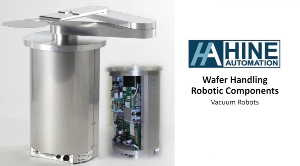
Atmospheric Robots: Operate in cleanroom air environments (60% of market)
Vacuum Robots: For processes requiring low-pressure conditions (35% of market)
Specialty Robots: Including cryogenic and high-temperature variants (5% of market)
By Application:
Wafer Transport: Moving wafers between tools and stations (40% share)
Process Handling: Directly involved in deposition, etching, and other processes (35% share)
Metrology & Inspection: Positioning wafers for measurement and quality control (25% share)
By Wafer Size:
200mm Wafer Systems: Still widely used for mature nodes (30% share)
300mm Wafer Systems: Dominant for advanced nodes (65% share)
Emerging 450mm Systems: Pilot lines and future development (5% share)
Geographically, the Wafer Handling Robots Market shows distinct regional characteristics. Asia-Pacific leads in volume (55% of installations), driven by massive fab investments in Taiwan, South Korea, and China. North America excels in innovation (40% of patents), while Europe maintains strength in precision subsystems and contamination control technologies.
Key Players and Competitive Landscape in the Wafer Handling Robots Market
The Wafer Handling Robots Market features a mix of established automation giants and specialized semiconductor equipment providers, each bringing unique strengths to this demanding sector.
Market Leaders:
Brooks Automation: Pioneer in vacuum robotics with 25% market share
Rorze Corporation: Japanese leader in high-speed atmospheric handlers
KUKA AG: Industrial automation giant expanding into semiconductor applications
Nidec Sankyo: Specialist in direct-drive wafer handling technology
JEL Corporation: Innovator in compact, modular robot designs
Emerging Challengers:
Robostar: Korean company making waves with AI-enhanced handling
Hirata Corporation: Developing novel contactless wafer transport systems
Innovative Robotics: Startup focusing on quantum-enhanced positioning
The competitive landscape is evolving rapidly as traditional Handling Robots manufacturers adapt their technologies for semiconductor applications. Recent years have seen significant M&A activity, with semiconductor equipment companies acquiring robotics specialists to vertically integrate their offerings.
Technological Innovations Driving the Wafer Handling Robots Market
The relentless push for smaller semiconductor nodes and larger wafer sizes continues to drive remarkable innovations in wafer handling technology.
Breakthrough Technologies:
Magnetic Levitation Drives: Eliminating mechanical wear in vacuum environments
AI-Powered Motion Optimization: Self-learning algorithms that reduce particle generation
Nanoscale Vibration Control: Active damping systems for atomic-layer deposition processes
Smart End Effectors: Grippers with real-time force and slip detection
Digital Twin Integration: Virtual simulations that predict real-world performance
Future-Focused Developments:
450mm Wafer Readiness: Next-generation platforms designed for larger wafers
Quantum Positioning Systems: Using quantum entanglement for nanometer-scale alignment
Self-Healing Materials: Robot surfaces that automatically repair minor damage
Energy Harvesting: Systems that recover and reuse kinetic energy
Perhaps the most significant trend is the integration of Wafer Handling Robots into broader Industry 4.0 ecosystems. Modern systems don't just move wafers - they collect vast amounts of process data, enable predictive maintenance, and even autonomously optimize fab workflows in real-time.
FAQs: Answering Key Questions About the Wafer Handling Robots Market
1. What factors should a semiconductor fab consider when selecting wafer handling robots?
Fab operators must evaluate several critical parameters: cleanroom compatibility (ISO Class 1 or better), positioning accuracy (typically <±50μm for most processes), throughput speed (wafers per hour), mean time between failures (MTBF >10,000 hours for premium systems), and upgradeability. Compatibility with existing equipment interfaces (SEMI standards) and available footprint are also crucial considerations. Leading fabs are increasingly prioritizing data integration capabilities as they implement smart manufacturing initiatives.
2. How does the cost structure of wafer handling robots compare to other industrial robots?
Wafer Handling Robots command premium pricing compared to conventional industrial robots due to their specialized requirements. While a standard articulated industrial robot might cost $50,000-$100,000, wafer robots range from $150,000 for basic atmospheric models to over $1 million for advanced vacuum systems with integrated metrology. The cost breakdown differs significantly too - where industrial robots spend ~30% of cost on the arm itself, wafer robots invest ~50% in precision components and contamination control systems. Maintenance costs are also higher (15-20% of initial cost annually vs. 5-10% for industrial robots) but justified by the critical nature of their operation.
3. What are the biggest challenges facing the wafer handling robots market?
The Wafer Handling Robots Market faces several unique challenges: (1) The transition to 450mm wafers requires complete redesigns of handling systems while maintaining backward compatibility, (2) Increasing process complexity demands robots that can handle fragile structures like FinFETs and GAA transistors without damage, (3) Supply chain disruptions have made certain precision components harder to source, and (4) The industry faces a shortage of engineers skilled in both robotics and semiconductor processes. Additionally, as nodes shrink below 2nm, quantum effects begin to impact even robotic operations, requiring entirely new approaches to wafer handling.
Market Drivers and Growth Opportunities in the Wafer Handling Robots Market
Several powerful forces are propelling expansion in the Wafer Handling Robots Market, creating numerous opportunities for manufacturers and investors alike.
Primary Growth Drivers:
Chip Demand Surge: Global semiconductor shortages have accelerated fab construction worldwide
Node Shrinkage: Each new process generation requires more precise handling solutions
Labor Challenges: Difficulty finding skilled cleanroom operators boosts automation demand
Yield Pressure: Even minor handling improvements can save millions in increased yields
Government Incentives: CHIPS Act and similar initiatives worldwide funding fab automation
Emerging Opportunities:
Advanced Packaging: Fan-out and 3D IC technologies require new handling approaches
Compound Semiconductors: GaN and SiC production needs specialized handling solutions
Memory Evolution: 3D NAND stacking creates unique robotic challenges
Photonic Integration: Handling delicate optical components opens new markets
Quantum Computing: Emerging need for cryogenic wafer handling systems
The Wafer Handling Robots Market is also benefiting from spillover into adjacent industries. Technologies developed for semiconductor applications are being adapted for flat panel display manufacturing, MEMS production, and even advanced pharmaceutical manufacturing - each representing potential new revenue streams for wafer robotics providers.
The Future of the Wafer Handling Robots Market: Trends to Watch
As we look toward 2025 and beyond, several transformative trends will reshape the Wafer Handling Robots Market:
Key Future Trends:
Collaborative Systems: Hybrid setups where robots and humans work in tandem on complex tasks
Edge AI Integration: On-robot processing for real-time decision making
Sustainable Designs: Energy-efficient systems with reduced consumable usage
Modular Architectures: Plug-and-play components for easier upgrades
Quantum-Enabled Robotics: Leveraging quantum phenomena for unprecedented precision
The Wafer Handling Robots Market stands at an exciting inflection point. No longer just mechanical movers, these systems are becoming intelligent, connected components of the semiconductor manufacturing ecosystem. As the industry pushes the boundaries of Moore's Law, wafer handling robotics will play an increasingly central role in making next-generation chips possible. For businesses operating in or adjacent to this space, understanding these dynamics isn't just interesting - it's essential for maintaining competitive advantage in the fast-evolving world of semiconductor manufacturing.