Imagine a world where a single speck of dust could derail technological progress. In the heart of semiconductor fabs, where nanoscale circuits power our phones, AI systems, and space exploration, microscopic contamination means catastrophic failure. Enter the unsung heroes – Wafer Handling Robots – hyper-specialized automation marvels ensuring flawless silicon journeys. This article pulls back the curtain on these precision engineers, revealing how AI advancements transform them from mechanical arms into cognitive systems critical for sustaining Moore's Law. Discover why they're the pivotal link between raw silicon and the artificial intelligence revolution.
What Are Wafer Handling Robots and Why Do They Matter in Semiconductor Fabs?
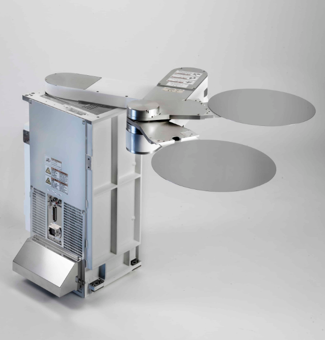
Wafer Handling Robots are ultra-clean, precision-engineered robotic systems designed exclusively for transporting semiconductor wafers between tools during chip manufacturing. Unlike standard industrial robots, they operate in ISO Class 1 cleanrooms (fewer than 12 particles per cubic meter), using specialized end-effectors that handle wafers without micro-scratches or electrostatic discharge. Their 6-axis articulated or linear designs achieve micron-level repeatability – positioning 300mm wafers within 20 microns of target locations, equivalent to placing a basketball within a soda can's rim from 50 feet away. Without them, producing advanced chips like NVIDIA's AI GPUs would be impossible.
The AI Acceleration Fuelling Smarter Wafer Transport
Traditional Wafer Handling Robots followed pre-programmed paths. Next-gen systems leverage machine learning to adapt in real-time. Computer vision algorithms scan wafers mid-transport to detect edge defects or warping that could cause misprocessing. Reinforcement learning optimizes path trajectories – reducing transit time by 35% while avoiding collisions in congested tool zones. Cloud-connected Wafer Handling Robots also predict maintenance needs using vibration sensors, cutting unplanned downtime by up to 50%. These AI integrations transform throughput in EUV lithography clusters where a single Handling Robot delay costs $20,000/hour in lost production.
Breakdown: How Modern Wafer Handling Robots Achieve Impossible Precision
Four technological pillars enable today's Wafer Handling Robots to manipulate billion-dollar wafer lots:
1. MagLev Drive Systems: Frictionless magnetic levitation transports eliminate particulates from lubricants – the #1 contamination source in legacy robots. Applied Materials' Centura platforms use this for <0.1nm positioning jitter.
2. Self-Calibrating Sensors: Embedded metrology lasers constantly measure wafer position, triggering micro-adjustments via piezoelectric actuators. KLA's robots achieve ±5μm accuracy after 100,000 cycles.
3. Predictive Contamination Control: Bernoulli grippers use air vortices to float wafers without contact, while ionizers neutralize static charges that attract nanoparticles.
4. Machine Learning Orchestrators: Neural networks analyze terabytes of transport logs to optimize acceleration profiles, preventing brittle ultra-thin wafers from cracking during high-speed transfers.
Quantifying the $32 Billion Impact: Why Fabs Can't Survive Without Them
Every major efficiency gain in semiconductor manufacturing traces back to advances in Wafer Handling Robots:
? Yield Protection: Human handling introduces 200+ defects per square meter. Automated wafer transport slashes this to <0.01 defects/m2, saving fabs $15M/month on 5nm node scrap rates.
? Utilization Breakthroughs: Robots enable "lights-out fabs" with 95% equipment uptime versus 65% in manual operations. TSMC credits its Material Handling Robots for achieving 24/7 production cycles critical for meeting AI chip demand.
? Miniaturization Enablers: As transistors shrink below 3nm, vibration control during handling becomes paramount. New adaptive dampening systems in Tokyo Electron's robots suppress resonance to 0.05g – essential for quantum tunneling prevention.
Emerging AI Capabilities Redefining Robotic Wafer Management
The convergence of physics-based models with deep learning is birthing cognitive handling systems:
Generative Adversarial Networks (GANs) simulate millions of potential wafer-drop scenarios to pre-train robots before deployment. Lam Research's AI simulators cut real-world training time from 3 weeks to 8 hours.
Federated Learning Swarms: Robots across global fabs share anonymized performance data (without exposing proprietary processes) to collectively improve defect detection algorithms. A 2025 SEMI study showed swarm-trained models reduced edge chipping by 42%.
The 2nm Horizon: Next-Gen Wafer Robotics Challenges
With chip geometries approaching atomic scales, handling constraints intensify:
Material Science Barriers: 1.5nm-thick 2D transistors require handling pressures below 0.1 Pascals. Current vacuum grippers exceed this 400x over. MIT's electroadhesion prototype offers a solution with controllable nano-Newton adhesion forces.
Quantum Locking Needs: Quantum chips demand cryogenic handling at -273°C. Brooks Automation is pioneering superconducting levitating robots that float wafers using quantum flux pinning.
FAQs: Decoding Wafer Handling Mysteries
Can Wafer Handling Robots Adapt to Irregular Chip Shapes?
With the rise of chiplets and heterogenous integration, non-rectangular dies now exist. Advanced Wafer Handling Robots like those from JEL Corporation use conformable end-effectors with micro-suction cup arrays that dynamically adjust to uneven geometries without stress concentration.
How Do Robots Prevent Cross-Contamination Between Wafers?
Self-cleaning protocols include UV-C sterilization cycles and atomic layer deposition coating chambers that renew protective films between wafer groups. Advanced fab systems quarantine robots exposed to high-risk materials using automated containment zones.
What Safety Measures Exist For Wafer Handling Robot Failures?
Triple-redundant control systems immediately freeze all motion if sensors detect abnormal torque. Emergency gas bearings deploy to levitate wafers mid-air if power fails, while faraday cage shielding protects against EMP events that could disrupt control signals.
Conclusion: The Unseen Catalysts of Technological Progress
Wafer Handling Robots epitomize the intersection of extreme engineering and AI – transforming from blind mechanical arms into cognitive systems that perceive, decide, and adapt. As semiconductor complexity escalates exponentially, these robots become not just tools but indispensable partners in creating the substrates powering artificial general intelligence. Their continued evolution represents one of industry's most profound yet underappreciated technological frontiers.